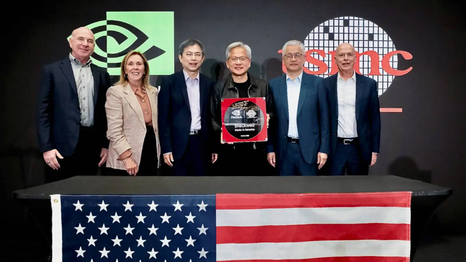
Phoenix, Arizona, hosted a milestone for the semiconductor industry: NVIDIA and TSMC announced the first U.S.-made silicon wafer built on the Blackwell architecture. NVIDIA CEO Jensen Huang attended the event and, together with TSMC vice president W. L. Wang, signed the first chip—an emblematic gesture marking the start of volume production.
TSMC Arizona will manufacture processors using 2–4 nm process technologies, including A16, aimed at artificial intelligence, telecommunications, and high-performance computing. Huang underscored the moment’s historical weight, noting that for the first time in a long while such a crucial chip is being produced in the United States, and he cast it as a key step in the country’s reindustrialization.
TSMC Arizona CEO Ray Chuang said the achievement is the result of decades of collaboration with NVIDIA and the efforts of local specialists. NVIDIA plans to apply its own AI and robotics to optimize future U.S. production sites and more tightly integrate these technologies into domestic manufacturing. It’s a signal that the wafer is more than a showpiece—the companies are treating production capability itself as a strategic asset.
More details about NVIDIA’s U.S. expansion and plans for AI infrastructure are expected at the NVIDIA GTC conference in Washington, scheduled for October 27–29.